Instruments
JEOL JXA-8530F Hyperprobe Electron Probe Microanalyzer (EPMA)
Location: LS 117 (Lab phone: 910-672-2037)
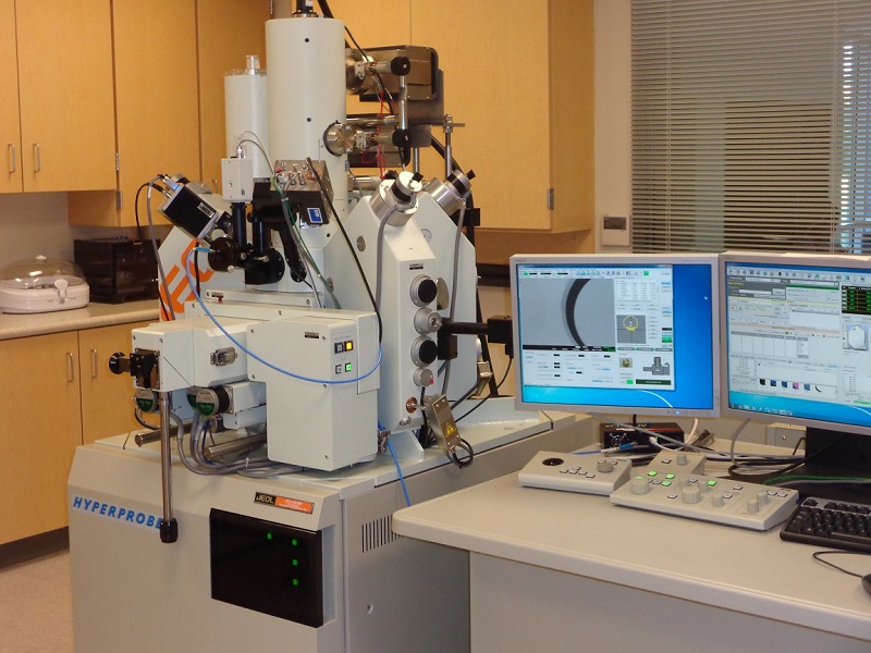
The JXA-8530F HyperProbe is a new generation EPMA featuring a field emission (FE) electron gun. The FE electron gun produces an extremely small spot size at a low accelerating voltage even with high probe currents (40 nm at 10 nA and 10 kV, 100 nm at 100 nA and 10 kV), allowing for WDS analyses with high X-ray spatial resolution. The microprobe is only 1/5 to 1/10 of the size produced in a thermionic-emission electron gun in conventional EPMA with tungsten filament or LaB6 tip.
This advanced instrument features with five WDS spectrometers with Rowland circle radius of 140 mm (140R) or 100 mm (100R), and each spectrometer contains 2 crystals as follows: Channel 1: TAP/LDE1; Channel 2: TAP/PETJ; Channel 3: TAP/LDE2; Channel 4: PETJ/LIF; and Channel 5: PETH/LIFH. The H type X-ray Spectrometer of 100R provides high X-ray intensity. Users can select from these spectrometers depending on their requirements. This instrument is attached with a JEOL 30 mm2 EDS silicon-drift detector (SDD). The high-count-rate SDD along with an in-situ variable aperture enables EDS analysis at WDS conditions. EDS spectra, maps and line scans can be acquired simultaneously with WDS data. In addition, two cathodoluminescence (CL) systems are installed on this instrument: Panchromatic Cathodoluminescence (PCL) System for imaging, and xCLent IV Advanced B Hyperspectral Cathodoluminescence System for both hyperspectral mapping and spectroscopy. More details can be found below. The remote controls of this instrument enable the user to operate the instrument remotely at a long distance. Key Features
| Secondary electron resolution | 3 nm |
| Detectable Element Range | Be to U |
| Detectable Wavelength Range | 0.087 to 9.3 nm |
| Number of X-ray Spectrometers | 1 to 5 (Plus EDS) |
| Specimen Size | 100 mm x 100 mm x 50 mm |
| X - Y Range | 90 mm x 90 mm |
| Accelerating Voltage | 1 - 30 kV (0.1 kV steps) |
| Probe Current Range | 10 pA to 500 nA |
| Minimum Probe Size | 40 nm diameter (10 kV, 10 nA) 100 nm diameter (10 kV, 100 nA) |
| Probe Current Stability | ±0.3 %/h (10 kV, 100 nA) |
| BEI (backscattered electron image) | Solid state, standard |
| Scanning Image Magnification | x 40 to 300,000 (WD: 11 mm) |
| Maximum Sample Size | 100 mm x 100 mm x 50 mm (H) |
For more details about the EPMA, visit JEOL website. Information about the cathodoluminescence systems: (1) Panchromatic Cathodoluminescence System - Imaging using wavelengths between 200 nm and 900 nm imaging simultaneously with SEI, BEI, EDS and up to 5 WDS detectors.
- Imaging using different bandpass filters selectively. (2) xCLent IV Advanced B Hyperspectral Cathodoluminescence System The xCLent is a fully integrated cathodoluminescence system for hyperspectral mapping and spectroscopy from 200 nm to 950 nm. The monochromatic CL system collects light through the FE-EPMA optical microscope. This allows the simultaneous collection of SE and BSE images as well as X-Rays from the WDS and EDS systems. When mapping, the entire CL spectra are stored in a hyperspectral cube for later data processing. This allows for later mapping of the specific wavelengths of interest, without any prior knowledge of the material. The CL detector does not require an additional specimen chamber port or limit the number of WDS spectrometers allowing for a full complement of 5 WDS spectrometers (no loss of a WDS spectrometer). - Scientific Grade spectrometer (Pro version) including 1024-element Hamamatsu linear CCD array.
- Peltier cooled detector with low noise and low dark signal.
- SpectraSuite Spectroscopy Platform Software for collection of cathodoluminescence spectra and alignment of optical system.
- Detector lens for CCD array.
- PCI Digital IO board for communications with EPMA and cabling.
- Software xClent Server IV for Windows to control/capture.
- Software xClent Image IV for visualization and interpretation of cathodoluminescence, X-ray and electron combined data.
- Luminescence database now includes over 2500 transitions.
- Cathodoluminescence database and Optical Fit (offline database). For more details about the EPMA, visit JEOL xCLent website.
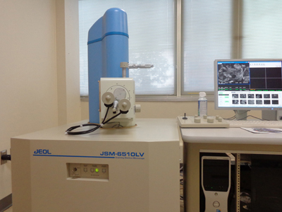
JEOL JSM-6510LV Scanning Electron Microscope (SEM)
Location: LS 130
Key Features
| Filament | Pre-centered W hairpin filament (with continuous auto bias) |
| Resolution | High Vacuum mode: 3.0 nm (30 kV), 8 nm (3 kV), 15 nm (1 kV) Low Vacuum mode: 4.0 nm (30 kV) |
| Accelerating voltage | 500 V to 30 kV |
| Magnification | x 5 to 300,000 (printed as a 128 mm x 96 mm micrograph) |
| LV Detector | Multi-segment BSED (std.) |
| LV Pressure | 10 to 270 Pa |
| Maximum specimen sizes | |
| LGS Type stage | Observable:125 mm diameter Loadable:152 mm Height:50 mm |
| Specimen stage | |
| LGS Type stage | Eucentric goniometer X = 80 mm, Y = 40 mm, Z = 5 mm-48 mm R = 360° (endless) Tilt -10/+90° |
| Frame Store | Up to 5120 × 3840 pixels |
| PC | Desktop, Windows 7 |
For more details, visit JEOL website.
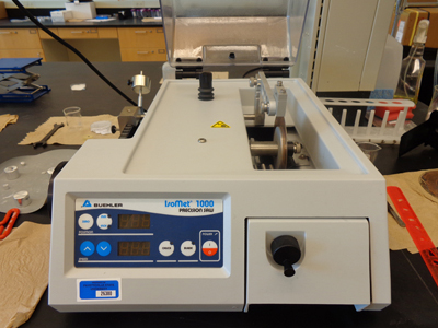
Buehler IsoMet® 1000 Precision Saw
Location: LSA 244
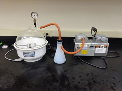
Buehler Cast N' Vac 1000 Vacuum Impregnation System
Location: LSA 244
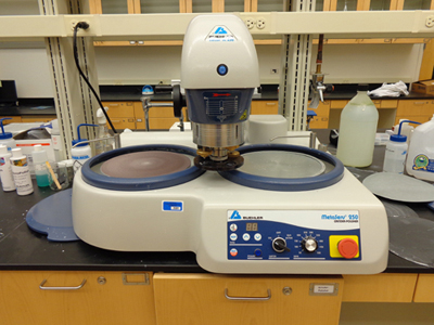
Buehler MetaServ® 250 Twin Grinder-Polisher with Vector LC 250 Power Head
Location: LSA 244
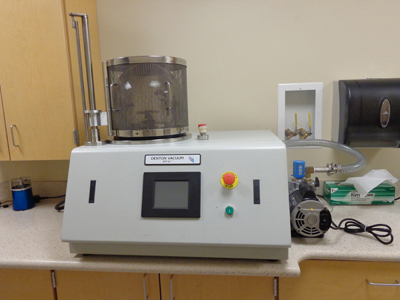
Denton Vacuum BTT-IV Evaporator
Location: LS 117
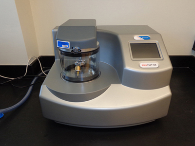
EMS 150T Turbo Pumped Sputter Coater/Carbon Coater
Location: LSA 244
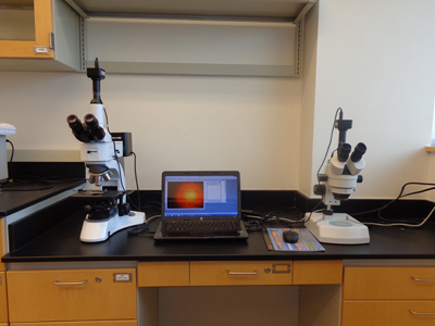
Metallurgical and Stereo Light Microscopes with CCD Cameras
Location: LSA 244

